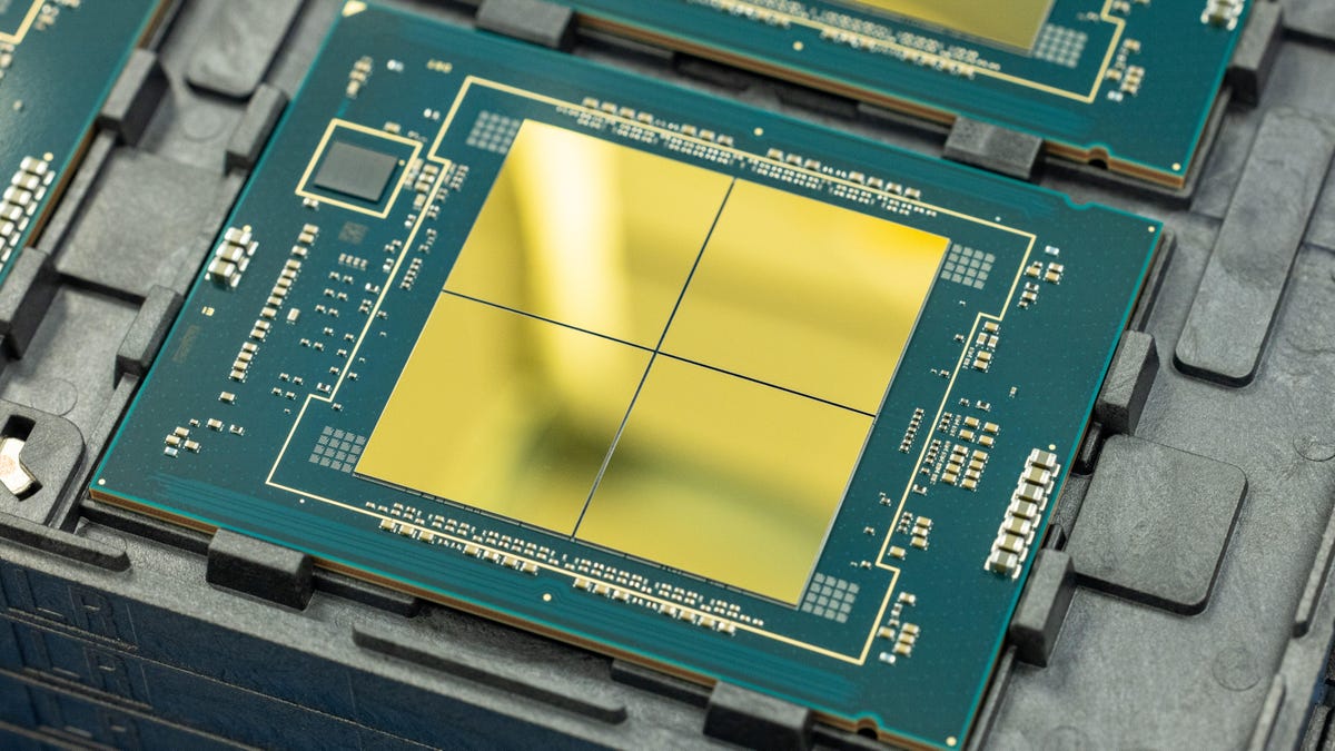
We knew that Intel’s Meteor Lake would begin an important new era with a design that stacks a few «chiplets» like pancakes into a single next-generation PC processor. But now we know something else: One of those chiplets will house a super low-power CPU that can keep a laptop ticking without as much of a hit on its battery.
Intel disclosed the new design detail at its Innovation conference Tuesday along with some details on Meteor Lake’s successors, Arrow Lake, Lunar Lake and Panther Lake. Chief Executive Pat Gelsinger also offered a status report on his multiyear effort to reclaim Intel’s lost processor design and manufacturing leadership. Meteor Lake, set to ship on Dec. 14 and for this year’s last crop of laptops, is a centerpiece of one phase of that effort.
Apple’s M series of processors, powering MacBook laptops with long battery life and no noisy cooling fans, have demonstrated the advantages of processor efficiency. Meteor Lake will fight back in two important ways, and if Intel delivers as promised, that should mean better laptops for millions of us who use Windows laptops.
See also: Inside Intel’s Chip Factory, I Saw the Future. It’s Plain Old Glass
First is an update to the main brain inside Meteor Lake’s design, a chiplet called the «compute tile» that includes a collection of CPU (central processing unit) cores. As with Intel’s current Alder Lake processors, formally called 13th-generation Core, the processor will include both big high-performance CPU cores for the most demanding tasks and smaller efficiency cores for lower-priority work and better battery life. Meteor Lake’s CPU cores have updated designs that are more efficient and that are built using the new Intel 4 manufacturing process that also is more efficient, Intel said.
But tucked into another tile, the system-on-a-chip (SOC) chiplet, there are even more efficient CPU cores on a «low power island.» The processor shuffles software tasks among the performance and efficiency cores many times each second to get the best results, and unused cores can be idled to save battery power.
«For best efficiency, you’ll see workloads bounced around the cores a lot,» said Tim Wilson, the engineering group vice president who led the SOC design. «For a lot of people, battery life today is as important as performance in their PC. Meteor Lake will shine on both.»
The chip also will bring new abilities to accelerate graphics on its graphics processing unit and artificial intelligence tasks on its neural processing unit. Both of those are key dimensions of performance in modern machines, particularly higher-end computers used for tasks like gaming or video and photo editing.
PCs aren’t powerful enough to run the highest-end large language models like ChatGPT, but AI technology is used for tasks like selecting photo subjects in Adobe Lightroom and removing backgrounds and audio noise in Microsoft Teams videoconferences.
New graphics brains for Meteor Lake
With the Meteor Lake processors, which the company will sell under the Core Ultra brand, Intel debuts its next generation of integrated graphics, Xe LPG. LPG operates more efficiently than the previous generation’s Xe LP, theoretically reaching higher frequencies at lower voltages for better battery life.
LPG also brings some important capabilities from the company’s Xe HPG discrete graphics to the GPU chiplet.
They include all the essentials for supporting DirectX 12 Ultimate: dedicated raytracing accelerators (one per graphics core, with up to eight cores per GPU) and support for mesh shaders, variable rate shading and sampler feedback.
The architecture also adds support for Intel’s upscaling technology, XeSS (Xe Super Sampling), which is partially dependent on AI. XeSS enables Endurance Gaming mode — an Intel-specific power-saving mode that combines aggressive upscaling with CPU throttling for those times when you desperately need to make it to a checkpoint on battery.
With LPG, laptops using Core Ultra chips get a boost to supporting a single 8K 60Hz with 10-bit HDR decoding and encoding or four 4K 60Hz HDR, 1440p 360Hz or 1080p 360Hz monitors, as well as HDMI 2.1.
TSMC, Intel’s competitor and partner
Intel is under fierce competitive pressure. During its years of stalled manufacturing progress, Taiwan Semiconductor Manufacturing Co. (TSMC) and Samsung leapfrogged Intel’s once formidable technology lead.
So did rivals that make chips. AMD made incursions into Intel’s market share, particularly in the server market where data centers are packed with thousands of high-end processors. Nvidia tapped into explosive demand for AI processors. And Apple dumped Intel processors, moving instead to its own M-series processors and offering compelling performance and lower power consumption. TSMC builds the processors for all three of those major Intel rivals.
But curiously, TSMC isn’t just an Intel competitor. It’s also a partner. It’s manufacturing most of the chiplets inside Meteor Lake.
TSMC is building Meteor Lake’s SOC tile — the chiplet that houses the low power island, AI accelerator, video decoder video and Wi-Fi system — on its N6 manufacturing process. That’s also used for the I/O tile, which handles input-output chores like Thunderbolt and USB connections.
TSMC’s more advanced N5 process is used to build Meteor Lake’s Arc GPU system. It will offer twice the performance and twice the performance per watt as the 13th-gen Alder Lake processors, Intel said.
Under Gelsinger, Intel is working on transforming its own chipmaking business by becoming a «foundry» like TSMC and Samsung that builds chips for other customers. It’s attracted a few clients, but the business isn’t expected to pick up in earnest until the Intel 18A manufacturing process arrives, scheduled for 2024.
Chiplets ahoy
Meteor Lake’s «disaggregated» design, enabled by an Intel chiplet-stacking technology called Foveros, is a sign of things to come for the processor industry.
AMD is stacking fast memory caches into its high-end PC processors, and Apple’s M2 Ultra consists of two M2 Max chips connected with a high-speed communication bridge. But Intel is more aggressive with its chiplet strategy, in part because of its need to try to catch up to competitors, Creative Strategies analyst Ben Bajarin said.

With the Sapphire Rapids Xeon chip for data centers Intel began selling earlier this year, then with Meteor Lake later this year, most of the company’s two main product lines will consist of processors made of several interlinked chiplets.
Packaging different chiplets increases manufacturing cost and time, but it also offers a variety of advantages. Different manufacturing processes can be used for different chiplets to optimize attributes like cost, power consumption and performance. And smaller chips are less prone to manufacturing defects.
And Intel’s glass substrate technology, also detailed at the Innovation conference, paves the way for even more advanced chiplet approaches. That glass — a foundation for the package that houses a processor — offers better speed, power and size advantages over today’s technology.
Meteor Lake doesn’t use glass substrates, which aren’t expected to arrive until later this decade, but it does illustrate Intel’s packaging skill. For example, to counteract the warping that means processors are slightly flexed like a potato chip, Intel uses variably sized solder balls to compensate and ensure good electrical contacts.
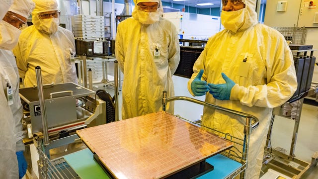
Intel also can use up to four types of solder balls in its process, for example judiciously employing more complex copper core balls for power connections. The company showed off this «multiball» technology in a tour of its advanced packaging research labs in Chandler, Arizona.
«As we look out into the next five to 10 years,» said Tom Rucker, the vice president in charge of Intel’s assembly integration work, «that packaging is going to become more important.»


